Do you know your PCBs are always manufactured on a large panel? Unless your PCB is large enough or needs special processing, it is likely produced on a large panel according to the order quantity.
If you need to produce PCBs in large quantities, it is best to make PCB panels. PCB manufacturer builds the PCB panel based on your PCB design. The PCBs are reasonably embedded in a large panel, which helps to achieve high production automation and repeatability, thereby improving production efficiency and reducing cost.
Benefits of panel creation
- Saving assembly cost with a PCB panel
Building multiple PCBs at one time can achieve maximum utilization of the substrate and can reduce overall manufacturing costs. Panelizing is a more cost-effective method of production.
- Improving the SMT assembly efficiency
A PCB panel is designed to help automate the fabrication and assembly process. And panel production allows all parts placed in one place for batch assembly without any additional setup time. This advantage is especially obvious in mass production.
- Reducing defects
Small PCBs are difficult to handle, but they can be paneled to improve manufacturing efficiency and reduce defects. And the panels better protect each PCB from shock vibration or mechanical stress. When laser stripping is used, these damages can even be completely avoided.
How to create a PCB panel?
PCB panel brings many benefits to PCB assembly manufacturing, but how to decide the panel size and panel type is important before panelizing. Because the assembly machine is limited in size, the PCB in the veneer or panel is too small or too large to be carried on the guide rail on the SMT line. And the panel size of PCB manufacturing is different from that of PCB assembly.
Although PCB designers can design their own panels, contract PCB manufacturers are usually recommended to do this work. PCB manufacturers have rich experience in panelization and understand the different requirements required, such as location, breakthrough spacing, and other panel functions. Then they can build and design more suitable panels based on size, shape, assembly standards, and expected yields.
Panel methods used in panel separation
After the manufacturing or assembly is completed, the PCBs eventually need to be separated from their panels into individual units. Manufacturers will add special features to the panel design to facilitate panel separation. Therefore, the layout designer should understand the requirements of these functions and provide necessary clearance to prevent damage to the circuits and components.
There are two main methods used in PCB panels to help board separation: V-cut and Tab-routing. Usually, a single PCB project will use the combination of V-cut and Tab-routing. It will increase PCB production cost but does reduce damages and PCBA separating labor.
V-cut

Tab-routing

Panel types used in PCB fabrication
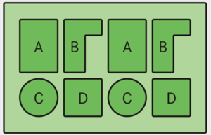
Each panel involves individual PCBs, which are arranged at a specific distance from each other according to the separation process. There are two different panel types in PCB fabrication:
- Homogenous composition (AAAAA):
Homogenous assembly means that only one type of PCB is produced per panel. This type of panel’s flexibility and effectiveness is much higher than any heterogeneous composition.

- Heterogeneous composition (ABCDE)
The heterogeneous panel is composed of different mixed types of PCBs. this panel type helps to reduce stocks and buffers, and it is more suitable for prototyping assembly
Conclusion
The panel design is not an easy task, many aspects must be considered in the design process. Especially the method of the separation process is critical to the design and maximum utilization of the panel.
ATAPCB will help you design panels based on the PCB assembly’s cost, quality, and profitability and optimize your panel design to get the highest quality of PCB assembly at a cost-effective price.