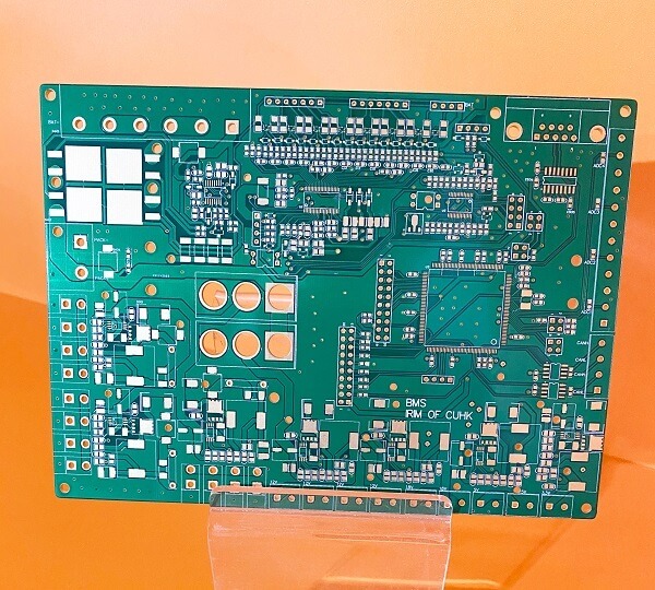
What is an HDI PCB?
HDI PCBs is the abbreviation of high density interconnect (HDI) printed circuit boards (PCBs). HDI micro via technology is the fastest growing technology in the PCB industry. HDI PCB has a higher circuit density per unit than a traditional PCB.
HDI PCBs are multilayer boards made by stacking method and micro-blind buried vias. The more times of lamination, the higher the technical grade of the circuit board. The ordinary HDI board is a one-time lamination, and high-grade HDI PCB uses two or more times lamination techniques. Not all buried vias are HDI PCBs. The PCBs are pressed twice after the blind hole plating can be called HDI boards.
The rapid development of high technology electronic design has put forward higher requirements for the performance and size of electronic products. Small is an everlasting pursuit from smartphones, smart wearable devices, and military equipment. HDI technology makes compact terminal products with higher standards of electronic performance and efficiency possible.
The advantages of HDI PCBs
- High circuit density
The micro via technology can embed interconnect wiring to the next layer without through-hole conductors. Therefore, the designers can place some pads on the surface of the outer panel to integrate more components. Then the PCB size can be reduced while increasing the density.
- Better electrical performance
Micro via interconnection technology helps to reduce signal reflection and crosstalk interference between circuits and increases the space of circuit design. And the micro via is small and short, which can reduce the influence of inductance, capacitance, and switching noise in signal transmission.
- Better thermal performance
HDI PCBs have better thermal properties because HDI dielectric has a higher glass transition temperature. Glass transition temperature (TG) indicates a temperature of the physical properties of the plastic become glassy or crystalline.
- Cost-effective
The PCB designers can reduce 8-layer through-hole PCBs to 4-layer HDI micro-hole technology package PCBs by using HDI technology during the design process. The wiring capability of the carefully designed HDI 4-layer PCB can achieve the same or better functionality as the standard 8-layer PCB. While micro-via processes increase the cost of HDI PCBs, proper design and reduction of layers can significantly reduce the cost of material and layers.
The applications and development prospects of HDI PCBs
Many electronic products have begun to develop in the direction of light, thin, short, and high density, which makes HDI PCBs grow very fast. HDI technology enables electronic products to have more functions, lighter weight, and smaller physical size while expanding technology, quality, and speed. HDI PCBs have been widely used in mobile phones, notebook computers, advanced digital cameras, automotive electronics, IC carrier boards, communication systems, aerospace, and medical products.
HDI PCBs are most widely used in mobile phones. In the next few years, the growth of global 5G mobile phones will increase exponentially, so the development prospects of HDI PCB are very impressive. And one of the most critical fields where HDI PCBs have made great progress in the medical field. Only HDI PCBs can provide the transmittance of a small package to meet high transmission in medical equipment like implants, emergency room monitors, CT scans, etc.
HDI PCBs capability from ATAPCB
HDI PCBs have very high manufacturing requirements. A minor defect or layout accident can also cause serious problems, so it is necessary to cooperate with PCB manufacturers with rich experience and advanced equipment.
ATAPCB is a leading supplier of HDI PCBs, and HDI PCBs manufacturing is one of our core manufacturing services. In order to provide higher-end HDI PCBs, ATAPCB attaches great importance to HDI material selection and manufacturing technology improvement. We have a professional production workshop and superb production technology to meet the most stringent requirements of HDI PCB manufacturing.


